Publications of Fraunhofer IISB

C. Kranert, C. Reimann, S. Kobayashi, Y. Ueji, K. Shimamoto, K. Omote
Scrutinising SiC with X-ray Topography
Cover Article of Compound Semiconductor, Volume 29, Issue 2, 2023

X-ray topography (XRT), already on the cusp of revolutionising the quantification of dislocations in SiC wafers, is now available in a high-throughput form that accelerates progress. The article describes how lab-scale XRT allows engineers to visualise single dislocations, thus making it possible to quantify them.     More info

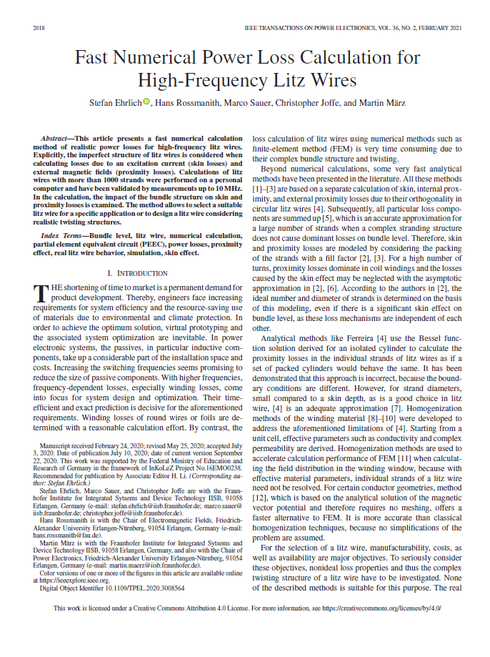
S. Ehrlich, H. Rossmanith, M. Sauer, C. Joffe, M. März
Fast Numerical Power Loss Calculation for High-Frequency Litz Wires
IEEE Transactions on Power Electronics 36 (2021) page 2018

The paper received a 2021 IEEE Transactions on Power Electronics First Place Prize Paper Award.

It presents a fast numerical calculation method of realistic power losses for high-frequency litz wires. Explicitly, the imperfect structure of litz wires is considered when calculating losses due to an excitation current (skin losses) and external magnetic fields (proximity losses). Calculations of complex litz wires were performed and have been validated by measurements. In the calculation, the impact of the bundle structure on skin and proximity losses is examined. The method allows one to select a suitable litz wire for a specific application or to design a litz wire considering realistic twisting structures.     More info

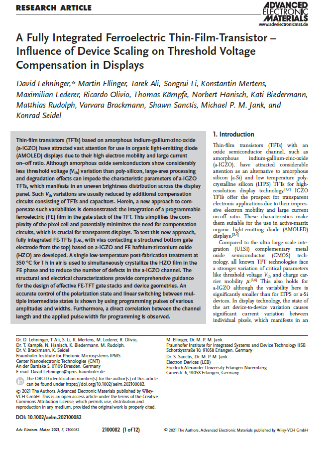
D. Lehninger, M. Ellinger, T. Ali, S. Li, K. Mertens, M. Lederer, R. Olivio, T. Kämpfe, N. Hanisch, K. Biedermann, M. Rudolph, V. Brackmann, S. Sanctis, M. Jank, K. Seidel
A Fully Integrated Ferroelectric Thin-film Transistor – Influence of Device Scaling on Threshold Voltage Compensation in Displays
Advanced Electronic Materials 7 (2021) 2100082

The paper was selected for the Hall of Fame collection of the journal

Thin-film transistors (TFTs) based on amorphous indium gallium zinc oxide (a-IGZO) have attracted vast attention for use in organic light-emitting diode displays. Large-area processing and degradation effects can impede the characteristic parameters of such TFTs. In the paper, the authors demonstrate a new method to compensate such variabilities: the integration of a programmable ferroelectric (FE) film in the gate stack of the TFT. To test this new approach, fully integrated FE-TFTs based on a-IGZO and FE hafnium zirconium oxide have been developed. The structural and electrical characterizations provide comprehensive guidance for the design of effective FE-TFT gate stacks and device geometries.     More info

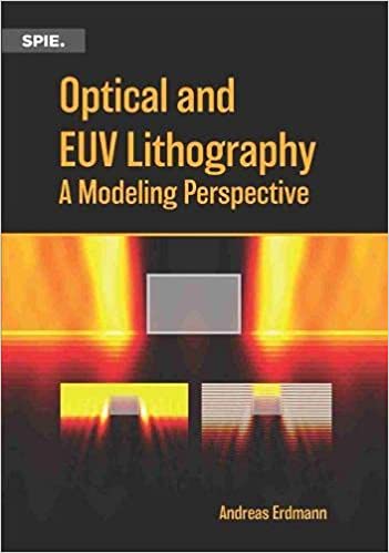
A. Erdmann
Optical and EUV Lithography - A Modeling Perspective
SPIE, 2021

The book by A. Erdmann, group manager at Fraunhofer IISB and renowned expert for lithography and optics, is intended to introduce students with backgrounds in physics, optics, computational engineering, mathematics, chemistry, material science, nanotechnology, and other areas to the fascinating field of lithographic techniques for nanofabrication. It is also suitable for helping senior engineers and managers expand their knowledge of alternative methods and applications. The material for the book was compiled during many years of lecturing on optical lithography technology, physical effects, and modeling at the Universität Erlangen-Nürnberg, as well as in preparation for dedicated courses on special aspects of lithography.     More info

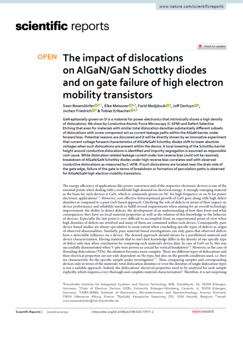
S. Besendörfer, E. Meissner, F. Medjdoub, J. Derluyn, J. Friedrich, T. Erlbacher
The Impact of Dislocations on AlGaN-GaN Schottky Diodes on Gate Failure of High Electron Mobility Transistors
Scientific Reports 10 (2020) 17252

The paper was published in the renowned Scientific Reports of the Nature Publishing Group

GaN epitaxially grown on Si is a material for power electronics that intrinsically shows a high density of dislocations. In the paper, it is shown by conductive atomic force microscopy (C-AFM) and defect selective etching that even for materials with similar total dislocation densities substantially different subsets of dislocations with screw component act as current leakage paths within the AlGaN barrier under forward bias. For AlGaN-GaN Schottky diodes, innovative methods are used to study the influence of these dislocations on the forward characteristics as well as on the breakdown behavior under high reverse bias.     More info

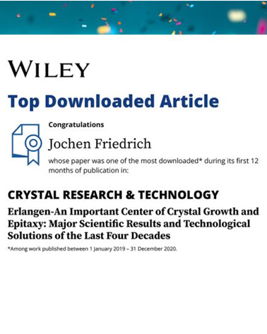
J. Friedrich, G. Müller
Erlangen – An Important Center of Crystal Growth and Epitaxy: Major Scientific Results and Technological Solutions of the Last Four Decades
Crystal Research and Technology 55 (2020) page 1900053

The paper is among the 10 most downloaded Wiley articles published between January 1, 2019 and December 31, 2020.

It describes the historic development of the Erlangen Crystal Growth Laboratory CGL, along with the essential developments and scientific achievements in the various fields of crystal growth and epitaxy. The CGL was founded by Prof. Georg Müller in 1974 at the Department of Material Science of the University of Erlangen-Nürnberg. Later, it became today's Materials Department of Fraunhofer IISB.     More info


Annual Reports

Overview of all IISB annual reports since 2000.


IISB-AKTUELL

IISB-AKTUELL informs about the latest developments at Fraunhofer IISB (in German).


Brochures & Flyers

Print products and information material from all our research areas for download as PDF.