 Fraunhofer Institute for Integrated Systems and Device Technology IISB
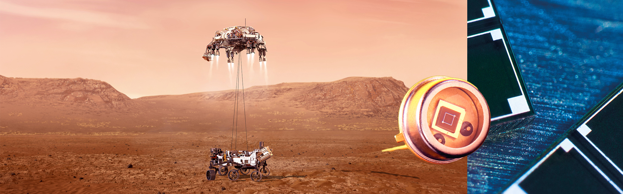
Sensor Technology with Silicon Carbide for Use in Space: UV Diodes on Mars Mission
When it comes to particularly low-loss semiconductor components and highly efficient power electronics, there is no way around silicon carbide (SiC) today. The wide-bandgap semiconductor material SiC is superior to conventional silicon in many respects and is conquering more and more new areas of application, for example in optoelectronics, sensor technology or solid-state quantum electronics. Even in space, SiC demonstrates its outstanding physical properties: A SiC UV photodiode from the Berlin-based company sglux is on board the current NASA mission Mars 2020. The SiC chip with the heterostructures for the UV photodiode was processed at Fraunhofer IISB in Erlangen on the institute's own CMOS line. Since the Mars rover “Perseverance” landed on the surface of Mars on February 18, 2021, the SiC photodiode has been functioning with absolute reliability under extreme environmental conditions. The UV sensor is a component of the SHERLOC deep-UV Raman spectrometer, employed by NASA to search for traces of past life on the surface of Mars. Fraunhofer IISB offers SMEs, mid-sized companies and industry low-threshold access to high-tech infrastructure and unique know-how in the field of semiconductor technology.
SiC – The New Silicon?
Driven by the energy transition and electromobility, there is currently a rapidly growing demand for electronic components for the particularly low-loss conversion of electrical energy. A prominent topic in semiconductor technology is therefore WBG or wide-bandgap semiconductors, such as silicon carbide, gallium nitride or aluminum nitride. They can handle high voltages at very low forward losses and thus offer the best prerequisites for building highly efficient power electronic systems.
Among WBG semiconductor materials, silicon carbide (SiC) has become particularly popular, and a wide range of commercial products is already available. In applications where the highest power densities and highest power conversion efficiencies are required, SiC devices with their superior electrical properties are already displacing conventional silicon power electronics. This is the case, for example, with the on-board networks and drive electronics of electric vehicles or the connection of renewable energy sources to the public power grid.
A Class of its Own
The special physical properties of the WBG semiconductor silicon carbide open up further interesting application options, such as in optoelectronics and sensor technology or for future solid-state quantum electronics. For example, the Berlin-based high-tech company sglux relied on SiC sensor components at an early stage and successfully established itself on the market with SiC photodiodes for measuring ultraviolet radiation (UV). These photodiodes are used wherever safety is a top priority. This is the case, for example, in medical technology for monitoring dialysis, in food processing for controlling sterilization processes, or in industry for controlling combustion processes.
The core components for the UV diodes, SiC chips with SiC heterostructures, are processed at Fraunhofer IISB in Erlangen, Bavaria, according to sglux specifications on the institute's own SiC CMOS line.
SiC Conquers Space

One of the most challenging operating environments for electronic components is certainly space. Here, all components must function absolutely reliably under extreme conditions, and even the smallest errors or failures can jeopardize the entire mission. Against this background, it is a great success for sglux GmbH from Berlin and also for Fraunhofer IISB that even NASA now belongs to the customer base of the SiC pioneers. During the current NASA mission MARS 2020, a SiC UV photodiode from sglux also landed on the red planet with the Mars rover "Perseverance" on February 18, 2021, and has been functioning reliably ever since.
The exceptional environment provides the perfect opportunity to demonstrate the reliability of sglux's products and the quality of the SiC sensors manufactured in small series at the IISB. "Perseverance" – which means endurance or tenacity – is the most advanced and elaborate rover NASA has ever sent to Mars. The roughly two-and-a-half billion dollar exploration vehicle is searching the Martian surface for traces of past microbial life and characterizing the planet's geology and climate, in preparation for a future manned Mars mission, among other things.
Life on Mars

Perseverance has a suite of state-of-the-art science instruments, among which a deep-UV Raman spectrometer attached to the rover's robotic arm plays a special role. Dubbed SHERLOC (Scanning Habitable Environments with Raman & Luminescence for Organics & Chemicals), the high-tech instrument is the first ever UV Raman spectrometer on Mars. There, it enables non-contact, spatially resolved and highly sensitive detection and characterization of organic matter and minerals on the surface and in the near subsurface. Meanwhile back on Earth, Raman spectroscopy, named after the physicist C. V. Raman, is used, for example, to study the material properties of semiconductor crystals.
Supported by a special camera called WATSON (Wide Angle Topographic Sensor for Operations and eNgineering) and a UV LASER, SHERLOC detects organic matter and minerals and creates topographic maps from them. Researchers on Earth then evaluate the measurement results and mineralogical maps to see if there is evidence of past water impact and signs of past life on Mars. Based on this, it will be decided which rock samples Perseverance should take and leave sealed in metal tubes on the surface of Mars for a future return to Earth (resample mission).
Ultimate Endurance Test

For its measurements, the UV Raman spectrometer uses a deep UV laser with a wavelength of 248.6 nm focused on a spot less than 100 µm in diameter. A SG01XL-5 SiC UV broadband photodiode from sglux is installed near the laser aperture, and detects the UV radiation power emitted by SHERLOC during spectral map measurements so that the laser output can be monitored when scanning the surface.
Before its use, sglux adapted the manufacturing process of this photodiode to its application and carried out elaborate selection, testing and characterization procedures. Subsequently, NASA subjected the candidates selected in this way to further tests and trials, for example on vibration resistance, behavior under strong acceleration, high-temperature resistance and alternating strength.
Unique Material Properties

Due to its unique properties, silicon carbide is currently the best semiconductor material for daylight-insensitive UV detectors and is ideal for use in difficult environments. The SiC-based photodiodes are almost completely blind to light in the visible wave range and impress with their high response speed. The small dark current in the femtoampere range ensures low noise, so that even very low UV radiation intensities can be measured reliably.
The SiC detectors tolerate comparatively high operating temperatures and operate stable in a temperature range from minus 55 to plus 170 °C. In this case, the temperature coefficient of the signal reaches values of less than 0.1 % per Kelvin and temperature-related changes in the measurement sensitivity can be compensated well. In addition, SiC has extreme radiation hardness, allowing the devices to retain their excellent electrical properties even when exposed to long and strong irradiation.
Economy and Science

New semiconductor materials such as silicon carbide always enable new applications. This gives newcomers and smaller companies in particular the opportunity to actively create value in the high-tech sector with innovative in-house developments. This commonly requires highly specialized key components that must be reliably available despite low quantities. SMEs and start-ups in particular often find it difficult to turn their brilliant ideas into marketable products due to a lack of in-house resources. However, competitive pressure is also increasing for medium-sized companies, and the investment required for technological progress is growing steadily. The big players, on the other hand, have little room for experimentation in their large production environments, where capacity utilization and yield take absolute priority.
Against this background, it is essential to offer SMEs, mid-sized companies and also industry low-threshold access to high-tech infrastructure and know-how in the field of semiconductor technology. Great successes are possible through collaboration between innovative companies like sglux and research institutes such as Fraunhofer IISB, as impressively demonstrated by the example of sglux's SiC UV diodes, which have traveled as far as Mars.
Dr.-Ing. Tilman Weiss, Managing Director of sglux GmbH, sums it up: "Our claim is that our UV sensors always last longer than the system in which they are installed. The mission to Mars so far is great confirmation of this fact, and also of our collaboration with Fraunhofer IISB. For the core of our products, we need precisely the technological expertise and system infrastructure available at the IISB. Only the symbiosis of entrepreneurship and research enables us to create sustainable value with exclusive products that are in demand worldwide."
Oleg Rusch, Group Manager SiC Bipolar Devices at Fraunhofer IISB, gives the following assessment: "Pure semiconductor manufacturing is not actually primary for the IISB, even though the processing of prototypes, special components and very small series is now part of our daily business. Our overall primary concern is to provide scientific excellence, process know-how and outstanding facility infrastructure to SMEs and industry. We see untapped potential for innovation at many companies that could be opened up with scientific support and R&D services in semiconductors."
SiC @ IISB
Fraunhofer IISB's activities in the area of integrated devices are deeply embedded in the institute's strategy of offering outstanding research services along the entire value chain – from semiconductor base materials to power electronic systems. The technological foundation for this is a continuous and industry-compatible CMOS process line for silicon and silicon carbide wafers up to 150 mm and 200 mm in diameter, respectively. As part of the joint initiative "Forschungsfabrik Mikroelektronik Deutschland" (FMD), semiconductor production is currently also being qualified for 200 mm SiC wafers. Within FMD, Fraunhofer IISB has positioned itself as a competence center for silicon carbide and is consistently expanding its activities in this field.
With its process line, the IISB also has access to advanced nanoscale heterointegration and patterning technologies. In addition, the technological portfolio is continuously being further developed with regard to assembly and connection technology and the reliability of electronic components and modules. The institute is thus expanding its range of products and services for highly reliable and highly efficient power electronics for use in extreme environmental conditions, such as those encountered in the aerospace industry.
Download / Links
Last modified: