Forschungsfabrik Mikroelektronik Deutschland (FMD) -
Research Fab Microelectronics Germany

Nationwide coordinated technology know-how from a single source

The Fraunhofer IISB is one of the 13 members of Forschungsfabrik Mikroelektronik Deutschland (FMD) - the largest cross-location R&D consortium for micro- and nanoelectronics in Europe with over 2000 scientists.

This innovative cooperation combines the advantages of two strong decentralized research organizations - the Fraunhofer-Gesellschaft and the Leibniz Association - with the synergies of a central organization to form the world's most efficient provider of applied research, development and innovation in the field of micro- and nanoelectronics. Thanks to its close integration and coherent appearance, FMD can thus offer not only customers from large-scale industry, but also SMEs and start-ups in particular, more comprehensive and easier access to the next generation of technology.

-> Homepage "Forschungsfabrik Mikroelektronik Deutschland" (FMD)


Locations of FMD in Germany
Process line for processing the backside of silicon carbide wafers for vertical power devices
© Kurt Fuchs / Fraunhofer IISB
Process line for processing the backside of silicon carbide wafers for vertical power devices

The Function of Fraunhofer IISB in the Research Factory Microelectronics Germany

Disco grinding and polishing machines for back-thinning and polishing of SiC wafers.
© Kurt Fuchs / Fraunhofer IISB
Disco grinding and polishing machines for back-thinning and polishing of SiC wafers.
X-ray topography system of the company Rigaku, model XRTmicron.
© Kurt Fuchs / Fraunhofer IISB
X-ray topography system of the company Rigaku, model XRTmicron.
High-Rate Xenon Plasma FIB (Focussed Ion Beam) System with Micro Pull Module.
© Kurt Fuchs / Fraunhofer IISB
High-Rate Xenon Plasma FIB (Focussed Ion Beam) System with Micro Pull Module.

The FMD is a global innovation driver which, as the largest multi-site R&D consortium for microelectronics in Europe, offers a unique diversity of competencies and infrastructure. FMD bridges the gap between basic research and customer-specific product development. In the field of power electronics, FMD's range of services includes the manufacture of power electronic devices and their integration into modules and systems. Special attention is paid to the manufacture and processing of Wide-Band-Gap (WBG) semiconductors, i.e. semiconductor materials with large band gaps (SiC, GaN, AlN, Diamond).

Within FMD, Fraunhofer IISB has a unique selling point with its integrated, certified production line for the processing of individual SiC-based prototype devices in an industry-compliant environment.

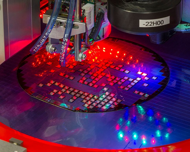
In the front-end area for wafer sizes of 100 mm and 150 mm, all desired process steps can be performed at Fraunhofer IISB, such as epitaxy, ICP dry etching, growth of silicon dioxide, aluminum implantation at elevated temperatures, activation tempering or conductive contact alloy. Usually, vertical components are manufactured in SiC for power electronics. Therefore, the processing of the backside of the SiC wafers is of critical importance. The FMD investments now also enable the bonding and debonding of already processed wafers, the thin grinding of wafers and the reduction of contact on the rear side by means of advanced metallization and laser silicidation.

New integration technologies and innovative assembly and system concepts for prototyping and the production of future power modules are available in the backend area. This makes it possible, for example, to realize particularly complex and compact structures, heavily stressed (special) applications with sometimes small quantities or durable high-temperature power electronic modules.

Extensive, complementary methods are available along the process chain for quality control. The most important of these are a fast, high-resolution X-ray topography system for the analysis of the structural properties of crystals, wafers and partially processed wafers and a combined surface inspection photoluminescence device for the analysis of the near-surface material properties of SiC along the process chain. The equipment is supplemented by special measuring stations, which are adapted to the specific, sometimes extreme conditions of power electronics, such as an extra-high voltage measuring station as well as special lifetime and reliability test laboratories.

For the research of new semiconductor materials with large band gaps, crystals of these materials are needed, which then have to be further processed into wafers in order to evaluate the potential in FMD for power electronics or for other applications such as in quantum technology. Since the new crystal materials, such as GaN, AlN or Diamond, are usually crystals with small diameters (50 mm or smaller), Fraunhofer IISB operates a special substrate and wafer laboratory to produce wafers from such crystals. The quality of the wafers used to manufacture the devices is tested using various analytical methods, including the determination of their epitaxial suitability and the production of special test structures.

Wafering Laboratory for New Wide-Bandgap Materials at Fraunhofer IISB

Aluminium Nitride Crystal
Cylindrical Grinding
Orientation
© Kurt Fuchs /Fraunhofer IISB
Orientation
Sawing
© Kurt Fuchs /Fraunhofer IISB
Sawing
Grinding
© Kurt Fuchs /Fraunhofer IISB
Grinding
 Polishing & Cleaning
© Kurt Fuchs /Fraunhofer IISB
Polishing & Cleaning
Epitaxy
© Kurt Fuchs / Fraunhofer IISB
Epitaxy
AlN Wafer
AlN Wafer

Backend of Line Processing for SiC @Fraunhofer IISB

Process Line for Wafer Thinning and Backside Contact Formation up to 150 mm.

Advanced Packaging Line for Power Electronics

The well-established, close-to-production processes for power semiconductors packaging and assembly such as stencil printing, die bonding, (vacuum) reflow, wire bonding and encapsulation are expanded to meet the demand of future technologies and systems driven by the ongoing miniaturization and advanced applications:

  • Joining layers, conductor circuits and windings can be processed with extended accuracy in positioning and volume by screen or stencil printers working on planar substrates.
  • Ink-jet printing enables high viscosity pastes and low viscosity inks to be applied over topography and complex 3D structures.
  • A high-precision die bonder positions components on substrates or on top of other components that are bonded/sintered in-situ or as batch (chip-2-wafer, chip-2-interposer, chip-2-chip, package-on-package).
  • A flexible sinter press allows single and double-sided sintering of large and small surfaces under inert or reactive gas atmospheres with tide mechanical and process tolerances and good reproducibility.   

The sustainable protection against environmental influences of components, substrates, modules and systems is completed by:

  • Well-established (vacuum) casting system allowing for the use of soft and hard encapsulation material as sealant
  • Flexible parylene coating system for conformal sealing with organic thin films as already established in medicine and avionics
  • Novel inorganic protective coatings with very high temperature and corrosion resistance

Innovative packaging concepts can be implemented with advanced processes:

  • additive production with 3D printers for ceramics, metal and polymer
  • Ultra-fine processing with ultra-short pulse laser and focused ion beam together with in-situ analytics

The advanced packaging line allows for the production of prototypes and pre-series in an ISO 7 clean room environment.

© Kurt Fuchs / Fraunhofer IISB
Stencil printer and Ink-jet printer for sinter and solder pastes as well as printing polymers and thermal interface materials in the packaging clean room
© Kurt Fuchs / Fraunhofer IISB
High-Rate Xe-Plasma Focussed Ion Beam Plant
© Fraunhofer IISB
High precision die bonder

Environmental Tests - Power Semiconductors – Devices and Systems

Laboratory for environmental tests of power semiconductor active and passive devices, smart modules and systems incl. wide-band gap material such as SiC for applications within power transmission, mobility, aerospace and industry.

The test conditions cover:   

  • Vibration
  • Temperature and humidity including temperature shock
  • Corrosive atmospheres e.g. corrosive gases and salt spray

and are accounting for the unique requirements of power semiconductors:

  • High power with high voltages and high currents
  • Avalanche-/breakdown and switching tests
  • Active cycling

Together with an experienced and state-of-the art failure analytics and characterization including:          

  • lock-in thermography and
  • focused-ion-beam / electron microscopy

both forensic studies as well as qualification tests are performed complying to industry standards such as AQG324.

© Kurt Fuchs / Fraunhofer IISB
Shaker Laboratory Laser Doppler Vibrometer Frequency response analysis of a printed circuit board with Laser Doppler Vibrometry on a shaker.
© Fraunhofer IISB
Active powercycling of wide-band-gap semiconductor
© Fraunhofer IISB
Corrosion in liquids and gasses